
Scanning electron microscope (SEM) picture of the reactor chamber region (right) and sniffer region (left). The position of the sniffer hole is indicated by the arrow to the left. (picture thanks to Toke)
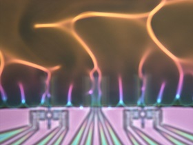
Micro discharge by Anpan. Defocused optical microscope picture of four-point-probes on 500-nm-thin silicon dioxide membranes.
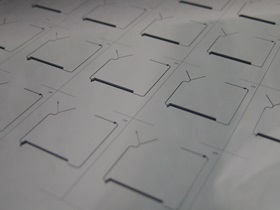
Microreactors fabricated on a silicon wafer. The reactors are diced out from the wafer before they are applied. (picture thanks to Toke)
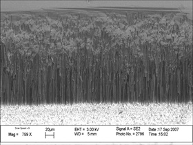
Nanoforest by Jordi. Up-side-down SEM picture of porous silicon.