Microstructural Analysis of Materials Processes in the SEM
About our Research
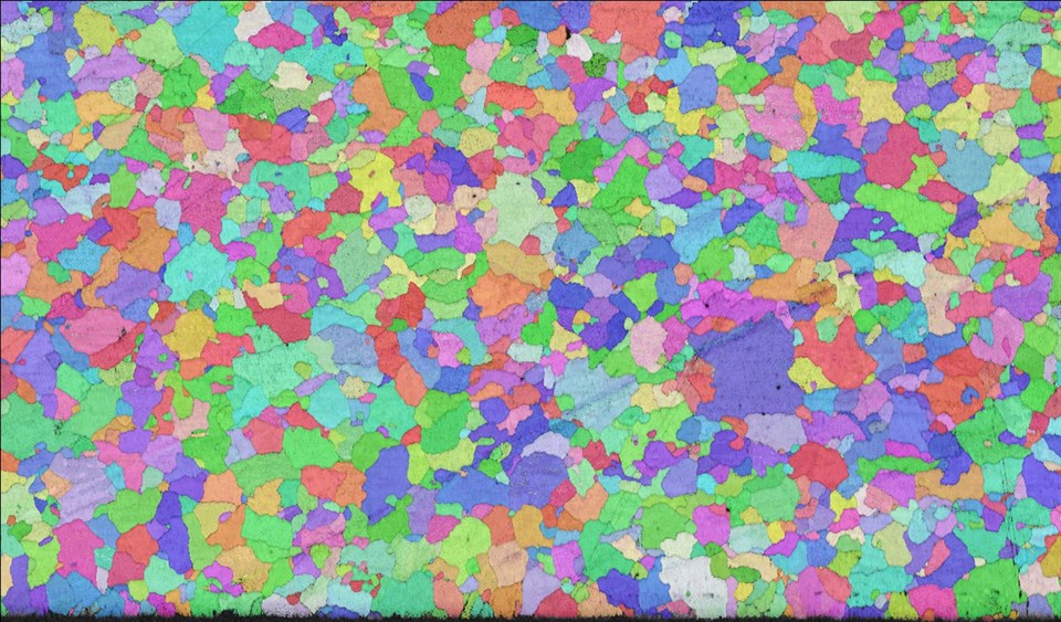
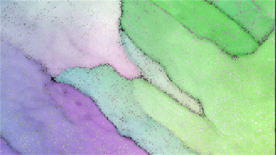
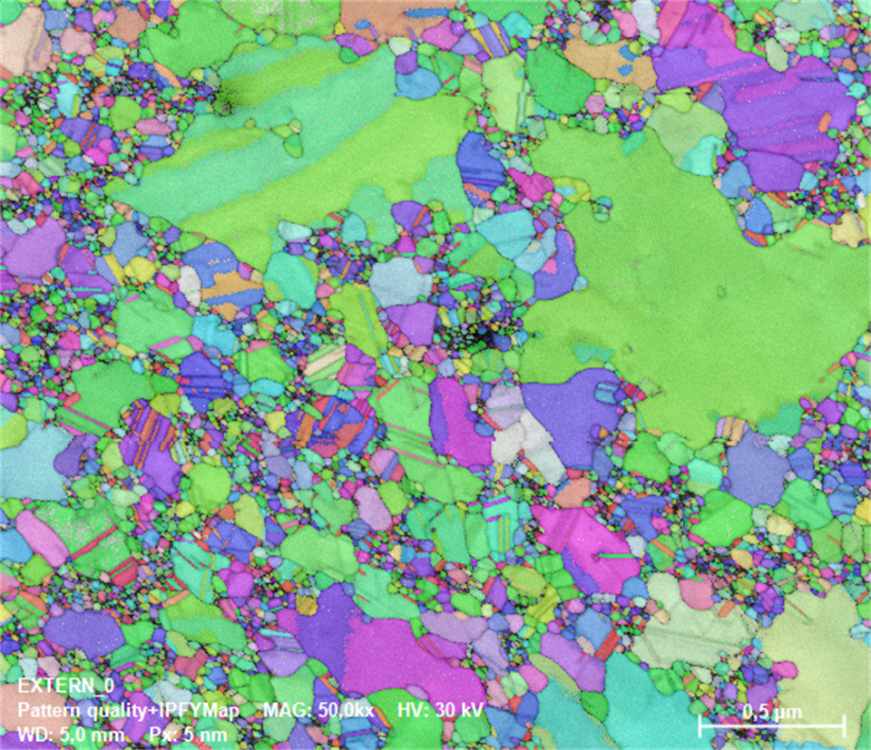
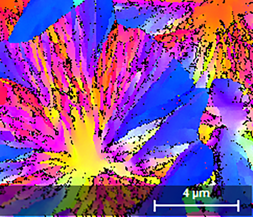
Our research group aims to understand materials properties, processes, structure and functionalities through high statistical microstructure characterization in the scanning electron microscope (SEM). Therefore, we focus on developing microscopy methods and solutions to enhance the potential of the SEM to solve materials challenges and understand its properties. In this context, we explore the versatility of the SEM (large specimen chamber, variable environment, multiple detectors and sources) as a link between the high-resolution structure information obtained in the transmission electron microscope (TEM) and the macroscopic properties of materials.
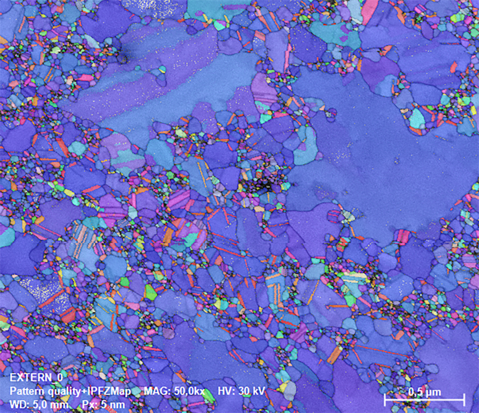
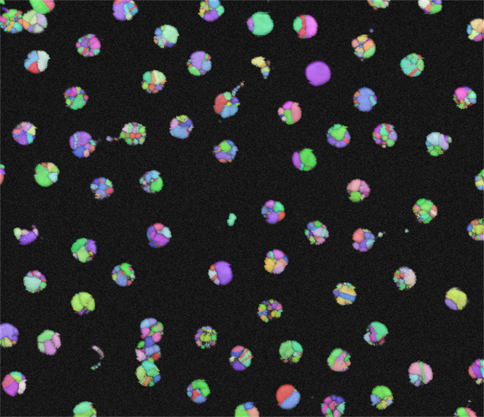
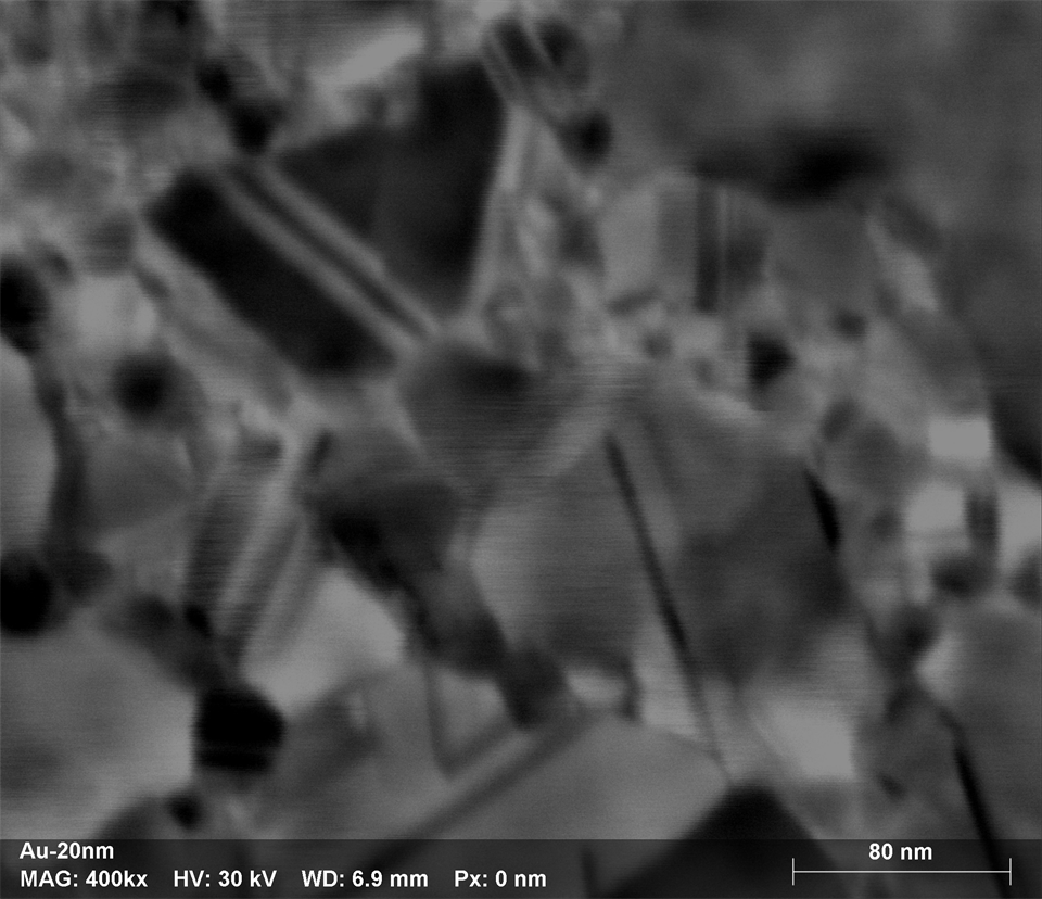
Our core competences lay in electron diffraction techniques (EBSD, 3D-EBSD, TKD and ECCI) which we often combine with elemental analysis (EDS) and focused ion beam to investigate bulk and electron transparent specimens with and without external stimulus such as heat. We are particularly interested in: (i) high throughput characterization of nanoparticles and thin films, (ii) understand microstructure formation and evolution in additive manufacturing processes, (iii) investigate microstructure evolution under rapid heating/cooling and under electrical biasing and (iv) low beam energy electron diffraction of 2D and beam sensitive materials.
