Innovation
Innovation, translating research results to tangible value creation, is built into the concept of DTU Nanolab. From the beginning in 1992 at that time called Mikroelektronik Centret, MIC, industry collaboration and spin-out of start-up companies was a major goal of the institute.

Innovation is built into Nanolab's concept
This concept has resulted in more than 30 spin out companies and was instrumental to build a micro/nano fabrication based industry in Denmark, where in 2019, just the five largest spin-outs had a turnover of more than 250 Mio Dkk and more than 250 employees.
In addition, DTU Nanolab is collaborating with several large international companies, where employees of these companies carry out R&D and, in some cases, also small-scale production in DTU Nanolab’s cleanroom.
The rules and tools of the semiconductor industry
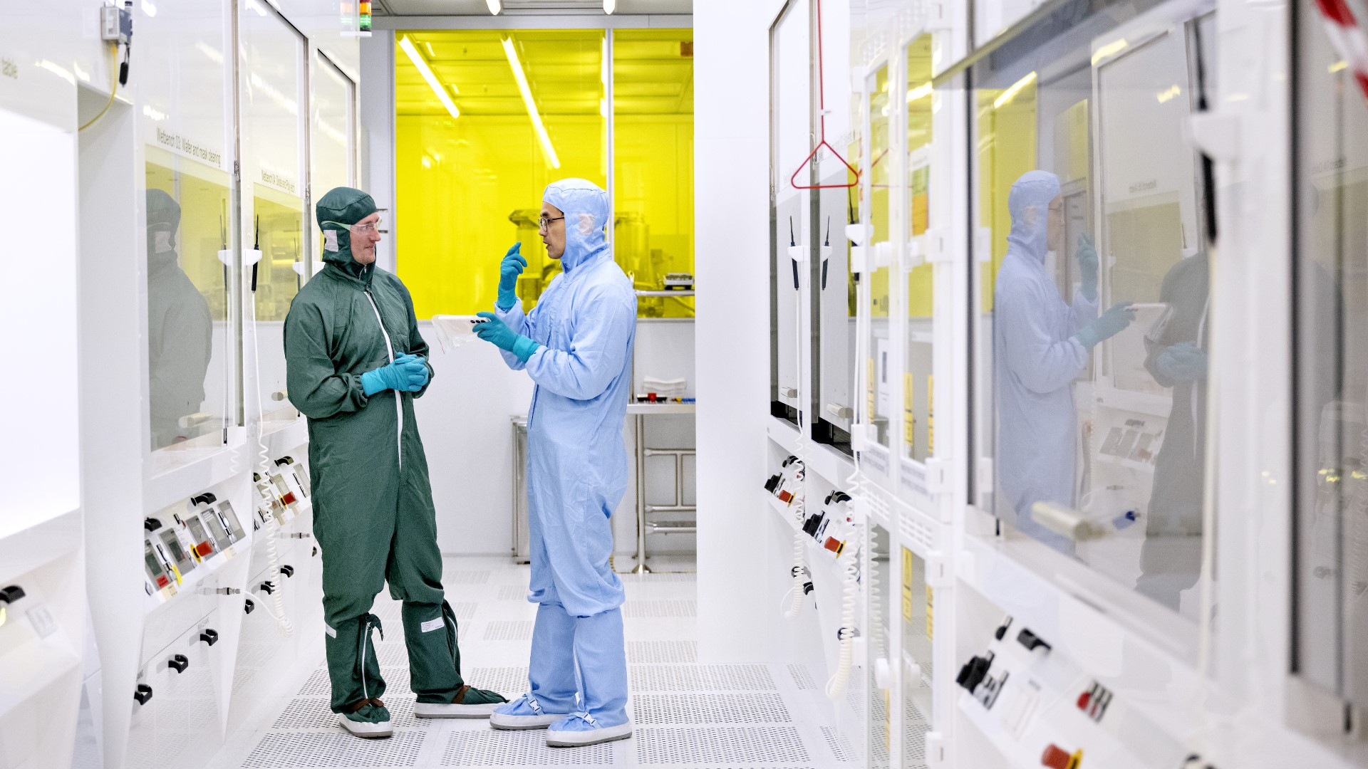
Although we do not fabricate electronics at DTU Nanolab, we are using the tools and processes that have their origin in the semiconductor industry.
Across all TRLs
AT DTU Nanolab we cover all Technology Readiness Levels, TRLs, from components for basic research on quantum technology to small scale chip production.
Micro and nanofabrication is fundamentally different in terms of innovation and scalability from other industrial sectors. While it requires a very expensive R&D and production setup the scalability is inherent as we typically deal with very small devices, developed and engineered on tools that are designed for mass fabrication.
What makes this industry special
A device typically has to go through many critical process steps, often more than 50. Each step requires a chemical and physical (plasma) process in a dedicated tool. Maintaining a yield of more than 99% on each of these steps, where a precision down to, in some cases few tenth of a nanometer, is required, is a challenge.
Developing such a process sequence and delivering a proof of concept can take years of research, as every process has to be established and finetuned on each of the tools.
To transfer these processes to a dedicated fabrication facility (e.g. an existing commercial wafer fab) will be extremely expensive and time consuming as every process step has to be readjusted on every tool.
Moreover, the capacity of such a fab will in almost all cases exceed the initial demand by a considerable factor. In many cases, these factors will lead to the breakdown of the business case that is already strained by a long and costly R&D.
What makes DTU Nanolab special
At DTU Nanolab we enable small scale production on the tools that has been finetuned and adjusted during the R&D process. This allows a direct production of the devices after successful proof of concept and prototyping without extra cost and delay. The fact that all our tools stem from the semiconductor fabrication, an industry that has been optimized for throughput for the last 60 years ensures ample capacity on these tools despite their co-use for research and production.
An example
As an example, many tools can process around 10 silicon wafers (with a diameter of e.g. 150 mm) per hour. It is not uncommon to get more than 1000 chips out of a wafer. For a high-end niche market a production capacity of 10 000 chips per hour will satisfy many business cases. Many companies run larger chips and have processes that do not reach these capacities but produce highly specialized, high value products into markets that can be satisfied with much less volume.
Keeping a production grade environment
Production yield is dependent on cleanliness and precision and can only be obtained by observing the highest standards at all times. Our facility is open 24/7, 365 days per year and all users have access at all hours. We have around 40 staff who do service and maintenance on the facility, the tools, develop processes, train new users and offer their expertise to all academic and industrial users. In order to maintain a high standard of quality and to ensure that we learn from our mistakes our cleanroom facility is ISO 9001:2015 certified.