Fabrication
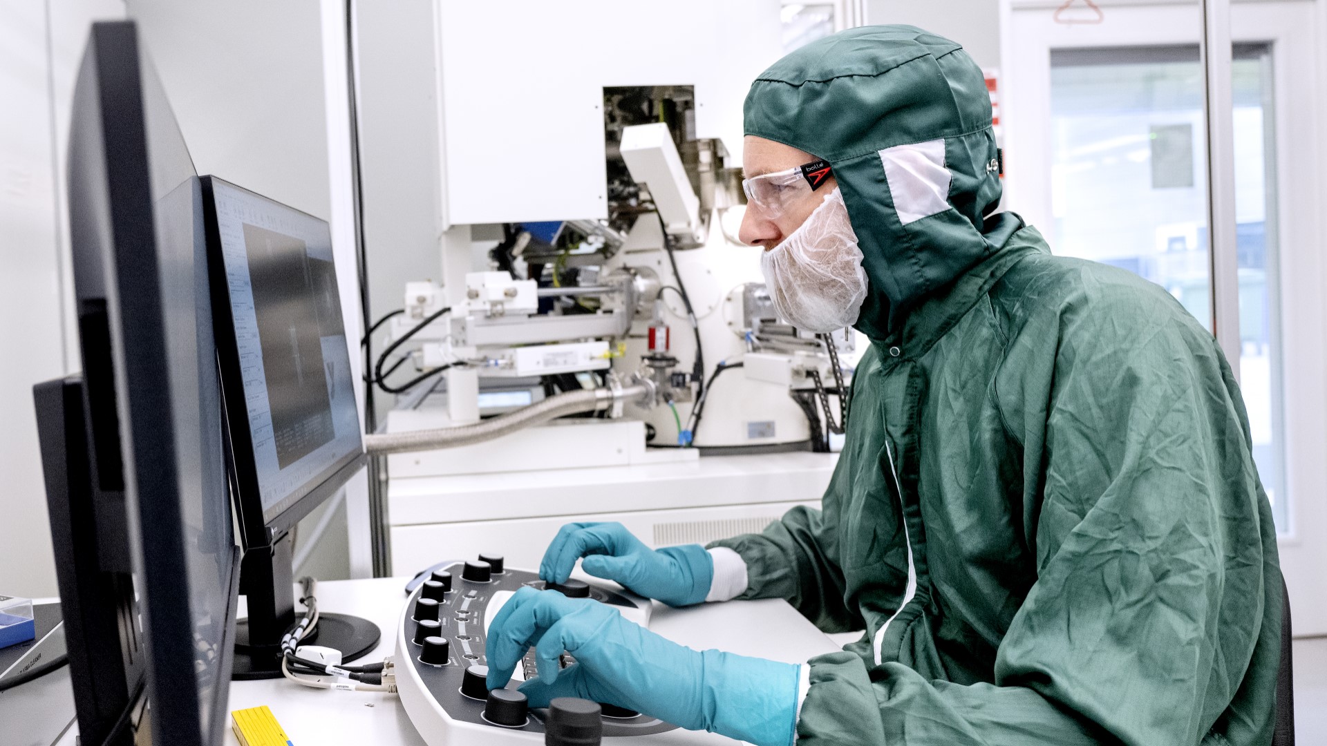
Cleanroom Fabrication facility specialized in state-of-the-art processes and techniques. Our facility offers a comprehensive range of capabilities to support your research and development needs.

Our cleanroom is equipped with advanced lithography systems, enabling precise patterning and mask alignment on a variety of substrates. Whether you require photolithography, electron beam lithography, or other advanced lithographic techniques, our skilled team and cutting-edge equipment ensure high-resolution and accurate fabrication of device structures.
We offer a wide range of etching processes to shape and define materials with exceptional precision. From wet chemical etching to plasma etching, we provide versatile etching capabilities for various materials, including semiconductors, metals, and dielectrics. Our expertise in etching techniques allows for controlled and reproducible removal of material layers to create intricate device features.
Quality control is paramount in device fabrication. Our cleanroom facility is equipped with in-line characterization tools for real-time monitoring and verification of critical parameters during the fabrication process. With advanced metrology techniques such as ellipsometry, spectroscopy, and profilometry, we ensure accurate and reliable measurements to validate your device performance.
We offer a wide range of deposition techniques, including physical vapor deposition (PVD), chemical vapor deposition (CVD), and atomic layer deposition (ALD). These techniques enable precise and controlled deposition of thin films, conformal coatings, and material layers with exceptional uniformity and adhesion. Our deposition capabilities cater to a diverse range of materials, including metals, oxides, nitrides, and organic compounds.
We understand the importance of packaging and integration for device functionality and reliability. Our cleanroom facility provides packaging solutions, including wire bonding, flip-chip bonding, encapsulation, and hermetic sealing. Our experienced team ensures proper handling and assembly of devices to meet your specific requirements, allowing for seamless integration and protection of your fabricated devices.
Our cleanroom supports fabrication using a wide range of materials, including silicon, III-V compounds, polymers, and more. With our extensive expertise and versatile equipment, we can accommodate various material systems, enabling the fabrication of diverse devices for applications in electronics, optoelectronics, sensors, and beyond.
At our Cleanroom Fabrication facility, we combine cutting-edge technologies, a controlled environment, and expert staff to deliver high-quality fabrication services tailored to your needs. Whether you are an academic researcher, industrial partner, or entrepreneur, we invite you to explore the possibilities and leverage our cleanroom capabilities to bring your innovative ideas to life.